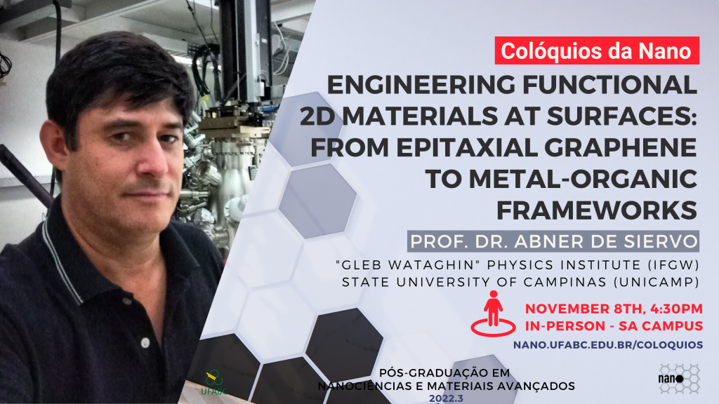
Palestrante: Prof. Dr. Abner De Siervo (IFGW/UNICAMP)
Resumo: The so-called 2D materials emerged in the last decades as an exciting new area for research that discovered new physics phenomena as well as plenty of room for technological applications. These materials can be divided into different classes that involve (1) one-atom-thick layer like the graphene “celebrity”, twisted graphene layers, and other members like h-BN, borophene, phosphorene, stanene, and so on; (2) layered materials like transition metal dichalcogenides (TMDs), and topological insulators; and (3) 2D functional organic-networks [1,2]. These materials have shown new interesting physical phenomena like linear-electronic dispersion, quantum-hall effect, outstanding photonic properties, unexpected magnetic, superconductor, ferroelectric, and piezoelectric behaviors [1,2]. All these physical phenomena have driven the community to propose applications for these materials in many different areas such as new supports for catalysts, supercapacitors, sensors, energy production (e.g solar cells) and storage, electronic and photonic devices, among others. Many of the interesting properties shown by 2D materials are attributed to the quantum confinement effects due to the reduced size in one dimension, i.e monolayer. Despite the wonderful possibilities, a bottleneck for applications with industrial-scale in some areas, for instance in the electronic industry, relies on a controllable way to produce large amounts of high-quality materials with specific characteristics, for instance, a large single-domain area of monolayer 2D material.
Título: Engineering functional 2D materials at surfaces: from epitaxial graphene to metal-organic frameworks
Data: 08/11/2022 – Auditório 801 – Bloco B, Santo André. Inscreva-se para certificados
Our group in Campinas has been working during the last years on the epitaxial growth of different members of these families (graphene, h-BN, h-BNC alloys, TMDs, and 2D-organic frameworks) [3-10] to better understand the electronic and atomic structure of these materials. In this seminar, I will show recent examples where we have applied different growth and functionalization strategies to produce epitaxial 2D materials. The electronic and atomic structure of these materials were characterized by combing different synchrotron-based techniques, such as x-ray photoemission and absorption spectroscopies with other surface science techniques, for instance, scanning tunneling microscopy and spectroscopy, as well as the support of theoretical calculations based on density-functional theory (DFT), to improve the understanding of the materials at an atomic scale.
References:
[1] Mengqi Zeng, et al. Chemical Reviews 118 (13), 6236-6296 (2018). [2] Akinwande, et al. Nature 573, 507–518 (2019). [3] L.H. de Lima et al., Physical Review B 87, 081403(R) (2013). [4] L.H. de Lima et al., Chemistry of Materials 26 (14), 4172-4177 (2014). [5] Rodrigo C.C. Ferreira et al., Chemistry of Materials 30 (20), 7201-7210 (2018). [6] M. Lepper et al., Angew. Chem. Int. Ed.. 57, 10074-10079 (2018). [7] Juan Carlos Moreno-López et al., Chemistry of Materials 31 (8), 3009-3017 (2019). [8] Alisson Ceccatto dos Santos, et al., Chemistry of Materials 32 (5), 2114-2122 (2020). [9] Gabriela Moura do Amaral, et al., Applied Surface Science, 538,148138 (2021). [10] Nataly Herrera-Reinoza, et al., Chemistry of Materials XX, xxxx-


